Cape Board Support
BeagleBone AI-64 has the ability to accept up to four EEPROM addressable expansion boards or capes stacked onto the expansion headers. The word cape comes from the shape of the expansion board for BeagleBone boards as it is fitted around the Ethernet connector on the main board. For BeagleBone this notch acts as a key to ensure proper orientation of the cape. On AI-64 you can see a clear silkscreen marking for the cape orientation. Most of BeagleBone capes can be used with your BeagleBone AI-64 also like shown in Fig-BeagleBone cape placement below.
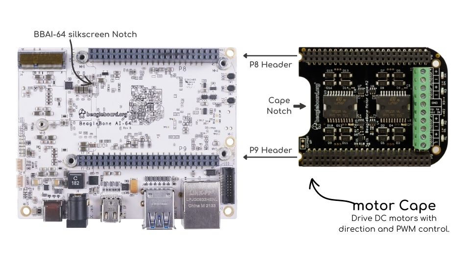
Fig-BeagleBone cape placement
This section describes the rules & guidelines for creating capes to ensure proper operation with BeagleBone AI-64 and proper interoperability with other capes that are intended to coexist with each other. Co-existence is not a requirement and is in itself, something that is impossible to control or administer. But, people will be able to create capes that operate with other capes that are already available based on public information as it pertains to what pins and features each cape uses. This information will be able to be read from the EEPROM on each cape.
For those wanting to create their own capes this should not put limits on the creation of capes and what they can do, but may set a few basic rules that will allow the software to administer their operation with BeagleBone AI-64. For this reason there is a lot of flexibility in the specification that we hope most people will find it liberating in the spirit of Open Source Hardware. On the other hand we are sure that there are others who would like to see tighter control, more details, more rules and much more order to the way capes are handled.
Over time, this specification will change and be updated, so please refer to the latest version of this manual prior to designing your own capes to get the latest information.
Warning
Do not apply voltage to any I/O pin when power is not supplied to the board. It will damage the processor and void the warranty.
BeagleBone AI-64 Cape Compatibility
The expansion headers on BeagleBone Black and BeagleBone AI-64 provides similar pin configuration options on P8 and P9 expansion header pins thus provide cape compatibility to a certain extent. Which means most BeagleBone Black capes will also be compatible with BeeagleBone AI-64.
Important
This section is still being worked on, please make sure you have the latest system reference manual (SRM).
EEPROM
Each cape must have its own EEPROM containing information that will allow the software to identify the board and to configure the expansion headers pins during boot as needed. The one exception is proto boards intended for prototyping. They may or may not have an EEPROM on them. An EEPROM is required for all capes sold in order for them operate correctly when plugged into BeagleBone AI-64.
The address of the EEPROM will be set via either jumpers or a dipswitch on each expansion board. Fig-Expansion board EEPROM without write protect below is the design of the EEPROM circuit.
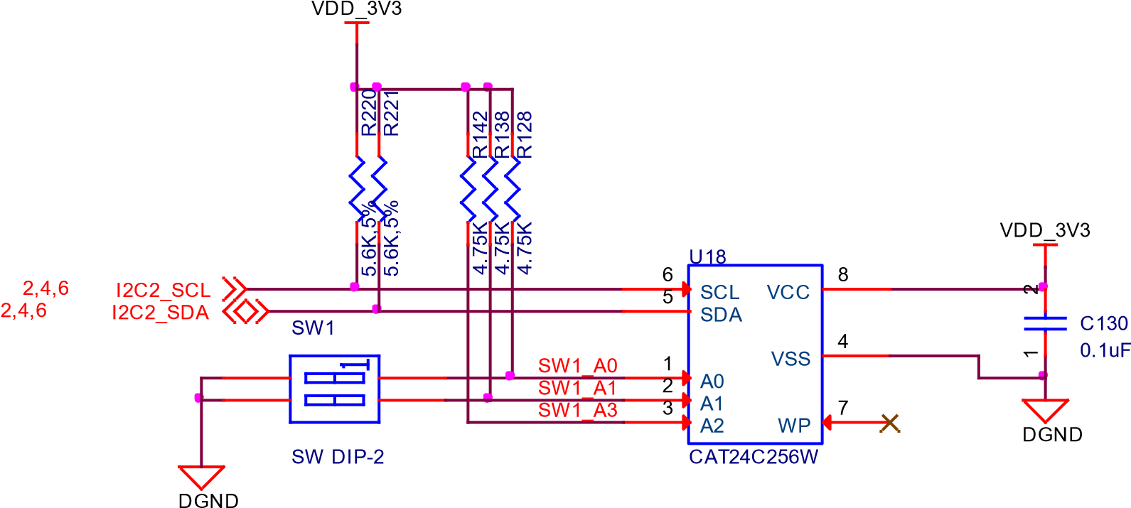
Fig-Expansion board EEPROM without write protect
The addressing of this device requires two bytes for the address which is not used on smaller size EEPROMs, which only require only one byte. Other compatible devices may be used as well. Make sure the device you select supports 16 bit addressing. The part package used is at the discretion of the cape designer.
EEPROM Address
In order for each cape to have a unique address, a board ID scheme is used that sets the address to be different depending on the setting of the dipswitch or jumpers on the capes. A two position dipswitch or jumpers is used to set the address pins of the EEPROM.
It is the responsibility of the user to set the proper address for each board and the position in the stack that the board occupies has nothing to do with which board gets first choice on the usage of the expansion bus signals. The process for making that determination and resolving conflicts is left up to the SW and, as of this moment in time, this method is a something of a mystery due to the new Device Tree methodology introduced in the 3.8 kernel.
Address line A2 is always tied high. This sets the allowable address range for the expansion cards to 0x54 to**0x57**. All other I2C addresses can be used by the user in the design of their capes. But, these addresses must not be used other than for the board EEPROM information. This also allows for the inclusion of EEPROM devices on the cape if needed without interfering with this EEPROM. It requires that A2 be grounded on the EEPROM not used for cape identification.
I2C Bus
The EEPROMs on each expansion board are connected to I2C2 on connector P9 pins 19 and 20. For this reason I2C2 must always be left connected and should not be changed by SW to remove it from the expansion header pin mux settings. If this is done, the system will be unable to detect the capes.
The I2C signals require pullup resistors. Each board must have a 5.6K resistor on these signals. With four capes installed this will result in an effective resistance of 1.4K if all capes were installed and all the resistors used were exactly 5.6K. As more capes are added the resistance is reduced to overcome capacitance added to the signals. When no capes are installed the internal pullup resistors must be activated inside the processor to prevent I2C timeouts on the I2C bus.
The I2C2 bus may also be used by capes for other functions such as I/O expansion or other I2C compatible devices that do not share the same address as the cape EEPROM.
EEPROM Write Protect
The design in Fig: Expansion board EEPROM with write protect has the write protect disabled. If the write protect is not enabled, this does expose the EEPROM to being corrupted if the I2C2 bus is used on the cape and the wrong address written to. It is recommended that a write protection function be implemented and a Test Point be added that when grounded, will allow the EEPROM to be written to. To enable write operation, Pin 7 of the EEPROM must be tied to ground.
When not grounded, the pin is HI via pullup resistor R210 and therefore write protected. Whether or not Write Protect is provided is at the discretion of the cape designer.
Variable & MAC Memory
VSYS_IO_3V3
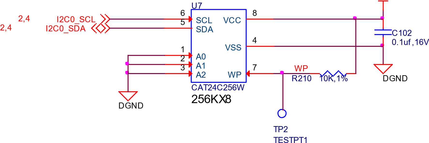
Fig: Expansion board EEPROM with write protect
EEPROM Data Format
Expansion Board EEPROM shows the format of the contents of the expansion board EEPROM. Data is stored in Big Endian with the least significant value on the right. All addresses read as a single byte data from the EEPROM, but two byte addressing is used. ASCII values are intended to be easily read by the user when the EEPROM contents are dumped.
Clean/Update table
Name |
Offset |
Size (bytes) |
Contents |
|---|---|---|---|
Header |
0 |
4 |
0xAA, 0x55, 0x33, 0xEE |
EEPROM Revision |
4 |
2 |
Revision number of the overall format of this EEPROM in ASCII =A1 |
Board Name |
6 |
32 |
Name of board in ASCII so user can read it when the EEPROM is dumped. Up to developer of the board as to what they call the board.. |
Version |
38 |
4 |
Hardware version code for board in ASCII.Version format is up to the developer.i.e. 02.1…00A1….10A0 |
Manufacturer |
42 |
16 |
ASCII name of the manufacturer. Company or individual’s name. |
Part Number |
58 |
16 |
ASCII Characters for the part number. Up to maker of the board. |
Number of Pins |
74 |
2 |
Number of pins used by the daughter board including the power pins used. Decimal value of total pins 92 max, stored in HEX. |
Serial Number |
76 |
12 |
Serial number of the board. This is a 12 character string which is: WWYY&&&&nnnn where, WW = 2 digit week of the year of production, YY = 2 digit year of production , &&&&=Assembly code to let the manufacturer document the assembly number or product. A way to quickly tell from reading the serial number what the board is. Up to the developer to determine. nnnn = incrementing board number for that week of production |
Pin Usage |
88 |
148 |
Two bytes for each configurable pins of the 74 pins on the expansion connectors, MSB LSB Bit order: 15..14 ….. 1..0 Bit 15….Pin is used or not…0=Unused by cape 1=Used by cape Bit 14-13…Pin Direction…..1 0=Output 01=Input 11=BDIR Bits 12-7…Reserved……..should be all zeros Bit 6….Slew Rate …….0=Fast 1=Slow Bit 5….Rx Enable…….0=Disabled 1=Enabled Bit 4….Pull Up/Dn Select….0=Pulldown 1=PullUp Bit 3….Pull Up/DN enabled…0=Enabled 1=Disabled Bits 2-0 …Mux Mode Selection…Mode 0-7 |
VDD_3V3B Current |
236 |
2 |
Maximum current in milliamps. This is HEX value of the current in decimal 1500mA=0x05 0xDC 325mA=0x01 0x45 |
VDD_5V Current |
238 |
2 |
Maximum current in milliamps. This is HEX value of the current in decimal 1500mA=0x05 0xDC 325mA=0x01 0x45 |
SYS_5V Current |
240 |
2 |
Maximum current in milliamps. This is HEX value of the current in decimal 1500mA=0x05 0xDC 325mA=0x01 0x45 |
DC Supplied |
242 |
2 |
Indicates whether or not the board is supplying voltage on the VDD_5V rail and the current rating 000=No 1-0xFFFF is the current supplied storing the decimal quivalent in HEX format |
Available |
244 |
32543 |
Available space for other non-volatile codes/data to be used as needed by the manufacturer or SW driver. Could also store presets for use by SW. |
Pin Usage
EEPROM Pin Usage shows the locations in the EEPROM to set the I/O pin usage for the cape. It contains the value to be written to the Pad Control Registers. Details on this can be found in section 9.2.2 of the TDA4VM Technical Reference Manual, The table is left blank as a convenience and can be printed out and used as a template for creating a custom setting for each cape. The 16 bit integers and all 16 bit fields are to be stored in Big Endian format.
Bit 15 PIN USAGE is an indicator and should be a 1 if the pin is used or 0 if it is unused.
Bits 14-7 RESERVED is not to be used and left as 0.
Bit 6 SLEW CONTROL 0=Fast 1=Slow
Bit 5 RX Enabled 0=Disabled 1=Enabled
Bit 4 PU/PD 0=Pulldown 1=Pullup.
Bit 3 PULLUP/DN 0=Pullup/pulldown enabled 1= Pullup/pulldown disabled
Bit 2-0 MUX MODE SELECT Mode 0-7. (refer to TRM)
Refer to the TRM for proper settings of the pin MUX mode based on the signal selection to be used.
The AIN0-6 pins do not have a pin mux setting, but they need to be set to indicate if each of the pins is used on the cape. Only bit 15 is used for the AIN signals.
+ |
+ |
+ |
15 |
14 |
13 |
12 |
11 |
10 |
9 |
8 |
7 |
6 |
5 |
|---|---|---|---|---|---|---|---|---|---|---|---|---|---|
Off set |
Conn |
Name |
Pin Usage |
Type |
+ |
Reserved |
+ |
+ |
S L E W |
R X |
P U - P D |
P U / D E N |
Mux Mode |
88 |
P9-22 |
UART2_RXD |
+ |
+ |
+ |
+ |
+ |
+ |
+ |
+ |
+ |
+ |
+ |
90 |
P9-21 |
UART2_TXD |
+ |
+ |
+ |
+ |
+ |
+ |
+ |
+ |
+ |
+ |
+ |
92 |
P9-18 |
I2C1_SDA |
+ |
+ |
+ |
+ |
+ |
+ |
+ |
+ |
+ |
+ |
+ |
94 |
P9-17 |
I2C1_SCL |
+ |
+ |
+ |
+ |
+ |
+ |
+ |
+ |
+ |
+ |
+ |
96 |
P9-42 |
GPIO0_7 |
+ |
+ |
+ |
+ |
+ |
+ |
+ |
+ |
+ |
+ |
+ |
98 |
P8-35 |
UART4_CTSN |
+ |
+ |
+ |
+ |
+ |
+ |
+ |
+ |
+ |
+ |
+ |
100 |
P8-33 |
UART4_RTSN |
+ |
+ |
+ |
+ |
+ |
+ |
+ |
+ |
+ |
+ |
+ |
102 |
P8-31 |
UART5_CTSN |
+ |
+ |
+ |
+ |
+ |
+ |
+ |
+ |
+ |
+ |
+ |
104 |
P8-32 |
UART5_RTSN |
+ |
+ |
+ |
+ |
+ |
+ |
+ |
+ |
+ |
+ |
+ |
106 |
P9-19 |
I2C2_SCL |
+ |
+ |
+ |
+ |
+ |
+ |
+ |
+ |
+ |
+ |
+ |
108 |
P9-20 |
I2C2_SDA |
+ |
+ |
+ |
+ |
+ |
+ |
+ |
+ |
+ |
+ |
+ |
110 |
P9-26 |
UAR*T1_RXD |
+ |
+ |
+ |
+ |
+ |
+ |
+ |
+ |
+ |
+ |
+ |
112 |
P9-24 |
UART1_TXD |
+ |
+ |
+ |
+ |
+ |
+ |
+ |
+ |
+ |
+ |
+ |
114 |
P9-41 |
CLKOUT2 |
+ |
+ |
+ |
+ |
+ |
+ |
+ |
+ |
+ |
+ |
+ |
116 |
P8-19 |
EHRPWM2A |
+ |
+ |
+ |
+ |
+ |
+ |
+ |
+ |
+ |
+ |
+ |
118 |
P8-13 |
EHRPWM2B |
+ |
+ |
+ |
+ |
+ |
+ |
+ |
+ |
+ |
+ |
+ |
120 |
P8-14 |
GPIO0_26 |
+ |
+ |
+ |
+ |
+ |
+ |
+ |
+ |
+ |
+ |
+ |
122 |
P8-17 |
GPIO0_27 |
+ |
+ |
+ |
+ |
+ |
+ |
+ |
+ |
+ |
+ |
+ |
124 |
P9-11 |
UART4_RXD |
+ |
+ |
+ |
+ |
+ |
+ |
+ |
+ |
+ |
+ |
+ |
126 |
P9-13 |
UART4_TXD |
+ |
+ |
+ |
+ |
+ |
+ |
+ |
+ |
+ |
+ |
+ |
128 |
P8-25 |
GPIO1_0 |
+ |
+ |
+ |
+ |
+ |
+ |
+ |
+ |
+ |
+ |
+ |
130 |
P8-24 |
GPIO1_1 |
+ |
+ |
+ |
+ |
+ |
+ |
+ |
+ |
+ |
+ |
+ |
132 |
P8-5 |
GPIO1_2 |
+ |
+ |
+ |
+ |
+ |
+ |
+ |
+ |
+ |
+ |
+ |
134 |
P8-6 |
GPIO1_3 |
+ |
+ |
+ |
+ |
+ |
+ |
+ |
+ |
+ |
+ |
+ |
136 |
P8-23 |
GPIO1_4 |
+ |
+ |
+ |
+ |
+ |
+ |
+ |
+ |
+ |
+ |
+ |
138 |
P8-22 |
GPIO1_5 |
+ |
+ |
+ |
+ |
+ |
+ |
+ |
+ |
+ |
+ |
+ |
140 |
P8-3 |
GPIO1_6 |
+ |
+ |
+ |
+ |
+ |
+ |
+ |
+ |
+ |
+ |
+ |
142 |
P8-4 |
GPIO1_7 |
+ |
+ |
+ |
+ |
+ |
+ |
+ |
+ |
+ |
+ |
+ |
144 |
P8-12 |
GPIO1_12 |
+ |
+ |
+ |
+ |
+ |
+ |
+ |
+ |
+ |
+ |
+ |
146 |
P8-11 |
GPIO1_13 |
+ |
+ |
+ |
+ |
+ |
+ |
+ |
+ |
+ |
+ |
+ |
148 |
P8-16 |
GPIO1_14 |
+ |
+ |
+ |
+ |
+ |
+ |
+ |
+ |
+ |
+ |
+ |
150 |
P8-15 |
GPIO1_15 |
+ |
+ |
+ |
+ |
+ |
+ |
+ |
+ |
+ |
+ |
+ |
152 |
P9-15 |
GPIO1_16 |
+ |
+ |
+ |
+ |
+ |
+ |
+ |
+ |
+ |
+ |
+ |
15 |
14 |
13 |
12 |
11 |
10 |
9 |
8 |
7 |
6 |
5 |
|||
|---|---|---|---|---|---|---|---|---|---|---|---|---|---|
Off set |
Conn |
Name |
Pin Usage |
Type |
+ |
Reserve |
+ |
+ |
S L E W |
R X |
P U - P D |
P U / DE N |
Mux Mode |
154 |
P9-23 |
GPIO1_17 |
|||||||||||
156 |
P9-14 |
EHRPWM1A |
|||||||||||
158 |
P9-16 |
EHRPWM1B |
|||||||||||
160 |
P9-12 |
GPIO1_28 |
|||||||||||
162 |
P8-26 |
GPIO1_29 |
|||||||||||
164 |
P8-21 |
GPIO1_30 |
|||||||||||
166 |
P8-20 |
GPIO1_31 |
|||||||||||
168 |
P8-18 |
GPIO2_1 |
|||||||||||
170 |
P8-7 |
TIMER4 |
|||||||||||
172 |
P8-9 |
TIMER5 |
+ |
+ |
+ |
+ |
+ |
+ |
+ |
+ |
+ |
+ |
+ |
174 |
P8-10 |
TIMER6 |
+ |
+ |
+ |
+ |
+ |
+ |
+ |
+ |
+ |
+ |
+ |
176 |
P8-8 |
TIMER7 |
+ |
+ |
+ |
+ |
+ |
+ |
+ |
+ |
+ |
+ |
+ |
178 |
P8-45 |
GPIO2_6 |
+ |
+ |
+ |
+ |
+ |
+ |
+ |
+ |
+ |
+ |
+ |
180 |
P8-46 |
GPIO2_7 |
+ |
+ |
+ |
+ |
+ |
+ |
+ |
+ |
+ |
+ |
+ |
182 |
P8-43 |
GPIO2_8 |
+ |
+ |
+ |
+ |
+ |
+ |
+ |
+ |
+ |
+ |
+ |
184 |
P8-44 |
GPIO2_9 |
+ |
+ |
+ |
+ |
+ |
+ |
+ |
+ |
+ |
+ |
+ |
186 |
P8-41 |
GPIO2_10 |
+ |
+ |
+ |
+ |
+ |
+ |
+ |
+ |
+ |
+ |
+ |
188 |
P8-42 |
GPIO2_11 |
+ |
+ |
+ |
+ |
+ |
+ |
+ |
+ |
+ |
+ |
+ |
190 |
P8-39 |
GPIO2_12 |
+ |
+ |
+ |
+ |
+ |
+ |
+ |
+ |
+ |
+ |
+ |
192 |
P8-40 |
GPIO2_13 |
+ |
+ |
+ |
+ |
+ |
+ |
+ |
+ |
+ |
+ |
+ |
194 |
P8-37 |
UART5_TX`+` |
+ |
+ |
+ |
+ |
+ |
+ |
+ |
+ |
+ |
+ |
+ |
196 |
P8-38 |
UART5_RX`+` |
+ |
+ |
+ |
+ |
+ |
+ |
+ |
+ |
+ |
+ |
+ |
198 |
P8-36 |
UART3_CTSN |
+ |
+ |
+ |
+ |
+ |
+ |
+ |
+ |
+ |
+ |
+ |
200 |
P8-34 |
UART3_RTSN |
+ |
+ |
+ |
+ |
+ |
+ |
+ |
+ |
+ |
+ |
+ |
202 |
P8-27 |
GPIO2_22 |
+ |
+ |
+ |
+ |
+ |
+ |
+ |
+ |
+ |
+ |
+ |
204 |
P8-29 |
GPIO2_23 |
+ |
+ |
+ |
+ |
+ |
+ |
+ |
+ |
+ |
+ |
+ |
206 |
P8-28 |
GPIO2_24 |
+ |
+ |
+ |
+ |
+ |
+ |
+ |
+ |
+ |
+ |
+ |
208 |
P8-30 |
GPIO2_25 |
+ |
+ |
+ |
+ |
+ |
+ |
+ |
+ |
+ |
+ |
+ |
210 |
P9-29 |
SPI1_D0 |
+ |
+ |
+ |
+ |
+ |
+ |
+ |
+ |
+ |
+ |
+ |
212 |
P9-30 |
SPI1_D1 |
+ |
+ |
+ |
+ |
+ |
+ |
+ |
+ |
+ |
+ |
+ |
214 |
P9-28 |
SPI1_CS0 |
+ |
+ |
+ |
+ |
+ |
+ |
+ |
+ |
+ |
+ |
+ |
216 |
P9-27 |
GPIO3_19 |
+ |
+ |
+ |
+ |
+ |
+ |
+ |
+ |
+ |
+ |
+ |
218 |
P9-31 |
SPI1_SCLK |
+ |
+ |
+ |
+ |
+ |
+ |
+ |
+ |
+ |
+ |
+ |
220 |
P9-25 |
GPIO3_21 |
+ |
+ |
+ |
+ |
+ |
+ |
+ |
+ |
+ |
+ |
+ |
+ |
+ |
+ |
15 |
14 |
13 |
12 |
11 |
10 |
9 |
8 |
7 |
6 |
5 |
Off set |
Conn |
Name |
Pin Usage |
Type |
Reserve |
S L E W |
R X |
P U - P D |
P U / DE N |
Mux Mode |
|||
+ |
+ |
+ |
+ |
0 |
0 |
0 |
0 |
0 |
0 |
0 |
0 |
0 |
0 |
222 |
P9-39 |
AIN0 |
+ |
+ |
+ |
+ |
+ |
+ |
+ |
+ |
+ |
+ |
+ |
224 |
P9-40 |
AIN1 |
+ |
+ |
+ |
+ |
+ |
+ |
+ |
+ |
+ |
+ |
+ |
226 |
P9-37 |
AIN2 |
+ |
+ |
+ |
+ |
+ |
+ |
+ |
+ |
+ |
+ |
+ |
228 |
P9-38 |
AIN3 |
+ |
+ |
+ |
+ |
+ |
+ |
+ |
+ |
+ |
+ |
+ |
230 |
P9-33 |
AIN4 |
+ |
+ |
+ |
+ |
+ |
+ |
+ |
+ |
+ |
+ |
+ |
232 |
P9-36 |
AIN5 |
+ |
+ |
+ |
+ |
+ |
+ |
+ |
+ |
+ |
+ |
+ |
234 |
P9-35 |
AIN6 |
+ |
+ |
+ |
+ |
+ |
+ |
+ |
+ |
+ |
+ |
+ |
Pin Usage Consideration
This section covers things to watch for when hooking up to certain pins on the expansion headers.
Expansion Connectors
A combination of male and female headers is used for access to the expansion headers on the main board. There are three possible mounting configurations for the expansion headers:
Single -no board stacking but can be used on the top of the stack.
Stacking-up to four boards can be stacked on top of each other.
Stacking with signal stealing-up to three boards can be stacked on top of each other, but certain boards will not pass on the signals they are using to prevent signal loading or use by other cards in the stack.
The following sections describe how the connectors are to be implemented and used for each of the different configurations.
Non-Stacking Headers-Single Cape
For non-stacking capes single configurations or where the cape can be the last board on the stack, the two 46 pin expansion headers use the same connectors. Fig-Single expansion connector is a picture of the connector. These are dual row 23 position 2.54mm x 2.54mm connectors.
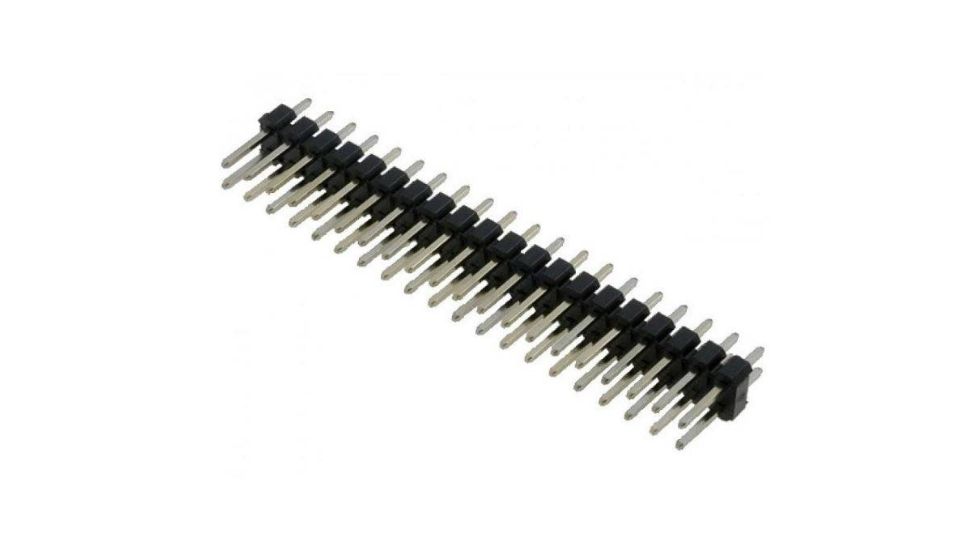
Fig-Single expansion connector
The connector is typically mounted on the bottom side of the board as shown in Fig-Single cape expansion connector on BeagleBone Proto Cape with EEPROM from onlogic . These are very common connectors and should be easily located. You can also use two single row 23 pin headers for each of the dual row headers.
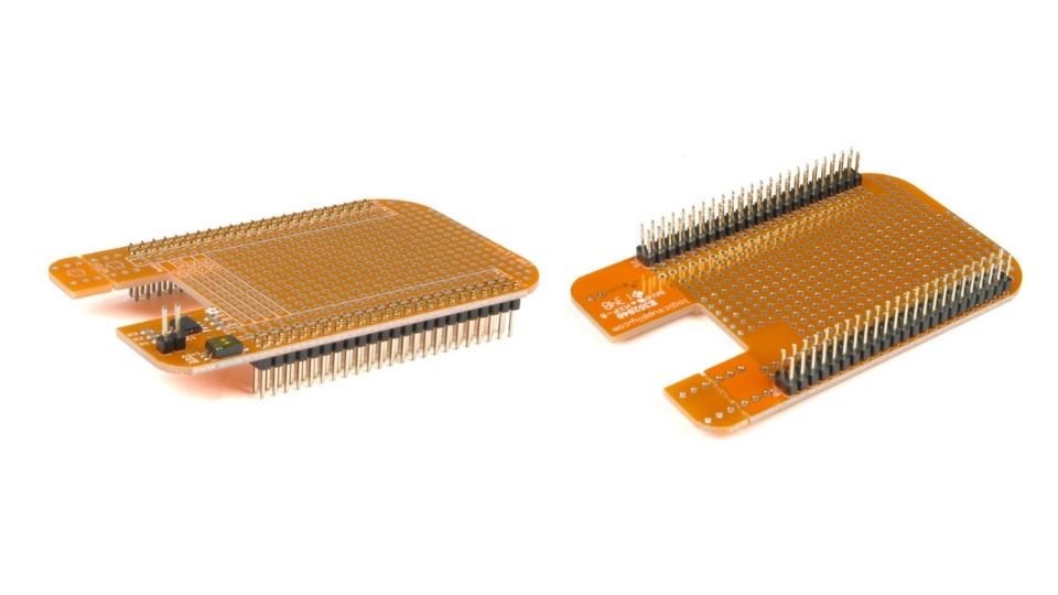
Fig-Single cape expansion connector on BeagleBone Proto Cape with EEPROM from onlogic
It is allowed to only populate the pins you need. As this is a non-stacking configuration, there is no need for all headers to be populated. This can also reduce the overall cost of the cape. This decision is up to the cape designer.
For convenience listed in Single Cape Connectors are some possible choices for part numbers on this connector. They have varying pin lengths and some may be more suitable than others for your use. It should be noted, that the longer the pin and the further it is inserted into BeagleBone AI-64 connector, the harder it will be to remove due to the tension on 92 pins. This can be minimized by using shorter pins or removing those pins that are not used by your particular design. The first item in**Table 18** is on the edge and may not be the best solution. Overhang is the amount of the pin that goes past the contact point of the connector on BeagleBone AI-64
SUPPLIER |
PARTNUMBER |
LENGTH(in) |
OVERHANG(in) |
|---|---|---|---|
TSHC-123-D-03-145-G-LF |
.145 |
.004 |
|
TSHC-123-D-03-240-G-LF |
.240 |
.099 |
|
TSHC-123-D-03-255-G-LF |
.255 |
.114 |
The G in the part number is a plating option. Other options may be used as well as long as the contact area is gold. Other possible sources are Sullins and Samtec for these connectors. You will need to ensure the depth into the connector is sufficient
Main Expansion Headers-Stacking
For stacking configuration, the two 46 pin expansion headers use the same connectors. Fig-Expansion Connector is a picture of the connector. These are dual row 23 position 2.54mm x 2.54mm connectors.
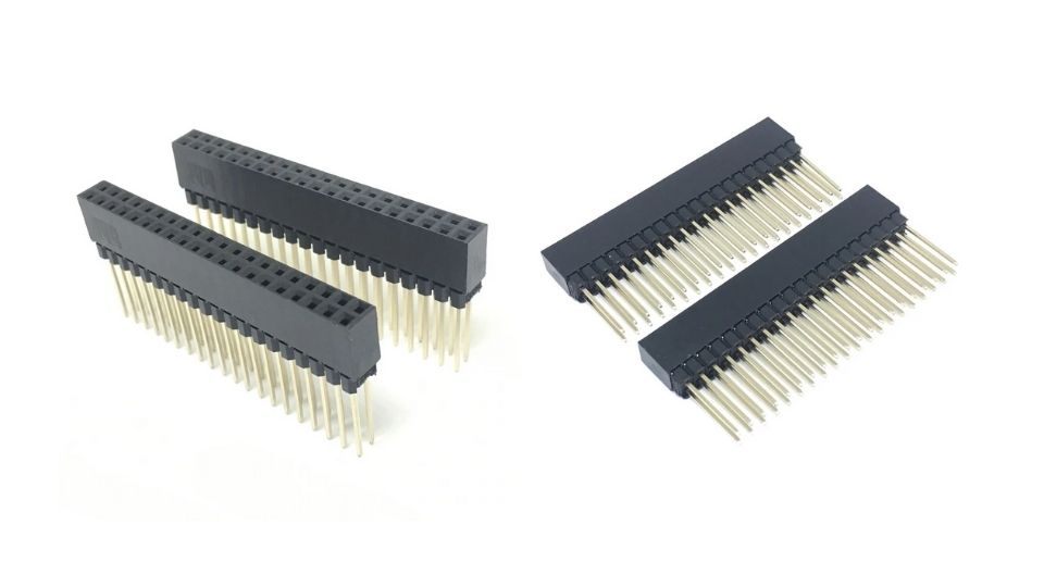
Fig-Expansion Connector
The connector is mounted on the top side of the board with longer tails to allow insertion into BeagleBone AI-64. Fig-Stacked cape expansion connector is the connector configuration for the connector.
Fig-Stacked cape expansion connector
For convenience listed in Table 18 are some possible choices for part numbers on this connector. They have varying pin lengths and some may be more suitable than others for your use. It should be noted, that the longer the pin and the further it is inserted into BeagleBone AI-64 connector, the harder it will be to remove due to the tension on 92 pins. This can be minimized by using shorter pins. There are most likely other suppliers out there that will work for this connector as well. If anyone finds other suppliers of compatible connectors that work, let us know and they will be added to this document. The first item in Table 19 is on the edge and may not be the best solution. Overhang is the amount of the pin that goes past the contact point of the connector on BeagleBone AI-64.
The third part listed in Stacked Cape Connectors will have insertion force issues.
SUPPLIER |
PARTNUMBER |
TAIL LENGTH(in) |
OVERHANG(in) |
|---|---|---|---|
SSHQ-123-D-06-G-LF |
.190 |
0.049 |
|
SSHQ-123-D-08-G-LF |
.390 |
0.249 |
|
SSHQ-123-D-10-G-LF |
.560 |
0.419 |
There are also different plating options on each of the connectors above. Gold plating on the contacts is the minimum requirement. If you choose to use a different part number for plating or availability purposes, make sure you do not select the “LT” option.
Other possible sources are Sullins and Samtec but make sure you select one that has the correct mating depth.
Stacked Capes w/Signal Stealing
Stacked with signal stealing expansion connector figure is the connector configuration for stackable capes that does not provide all of the signals upwards for use by other boards. This is useful if there is an expectation that other boards could interfere with the operation of your board by exposing those signals for expansion. This configuration consists of a combination of the stacking and nonstacking style connectors.
Stacked with signal stealing expansion connector figure
Retention Force
The length of the pins on the expansion header has a direct relationship to the amount of force that is used to remove a cape from BeagleBone AI-64. The longer the pins extend into the connector the harder it is to remove. There is no rule that says that if longer pins are used, that the connector pins have to extend all the way into the mating connector on BeagleBone AI-64, but this is controlled by the user and therefore is hard to control. We have also found that if you use gold pins, while more expensive, it makes for a smoother finish which reduces the friction.
This section will attempt to describe the tradeoffs and things to consider when selecting a connector and its pin length.
BeagleBone AI-64 Female Connectors
Connector Pin Insertion Depth shows the key measurements used in calculating how much the pin extends past the contact point on the connector, what we call overhang.
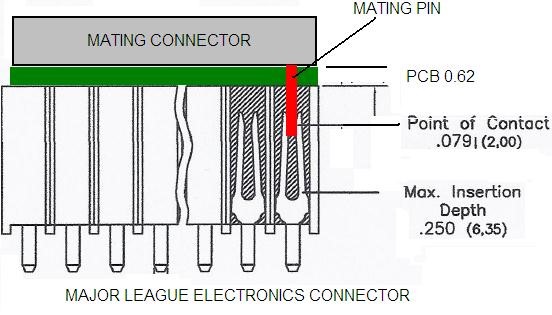
Connector Pin Insertion Depth
To calculate the amount of the pin that extends past the Point of Contact, use the following formula:
Overhang=Total Pin Length- PCB thickness (.062) - contact point (.079)
The longer the pin extends past the contact point, the more force it will take to insert and remove the board. Removal is a greater issue than the insertion.
Signal Usage
Based on the pin muxing capabilities of the processor, each expansion pin can be configured for different functions. When in the stacking mode, it will be up to the user to ensure that any conflicts are resolved between multiple stacked cards. When stacked, the first card detected will be used to set the pin muxing of each pin. This will prevent other modes from being supported on stacked cards and may result in them being inoperative.
In Connectors section of this document, the functions of the pins are defined as well as the pin muxing options. Refer to this section for more information on what each pin is. To simplify things, if you use the default name as the function for each pin and use those functions, it will simplify board design and reduce conflicts with other boards.
Interoperability is up to the board suppliers and the user. This specification does not specify a fixed function on any pin and any pin can be used to the full extent of the functionality of that pin as enabled by the processor.
DO NOT APPLY VOLTAGE TO ANY I/O PIN WHEN POWER IS NOT SUPPLIED TO THE BOARD. IT WILL DAMAGE THE PROCESSOR AND VOID THE WARRANTY.
NO PINS ARE TO BE DRIVEN UNTIL AFTER THE SYS_RESET LINE GOES HIGH.
Cape Power
This section describes the power rails for the capes and their usage.
Main Board Power
The Expansion Voltages describes the voltages from the main board that are available on the expansion connectors and their ratings. All voltages are supplied by connector**P9**. The current ratings listed are per pin.
Current |
Name |
P9 |
P9 |
Name |
Current |
|---|---|---|---|---|---|
250mA |
VDD_3V3B |
3 |
4 |
VDD_3V3B |
250mA |
1000mA |
VDD_5V |
5 |
6 |
VDD_5V |
1000mA |
250mA |
SYS_5V |
7 |
8 |
SYS_5V |
250mA |
The VSYS_IO_3V3 rail is supplied by the LDO on BeagleBone AI-64 and is the primary power rail for expansion boards. If the power requirement for the capes exceeds the current rating, then locally generated voltage rail can be used. It is recommended that this rail be used to power any buffers or level translators that may be used.
DC_VDD_5V is the main power supply from the DC input jack. This voltage is not present when the board is powered via USB. The amount of current supplied by this rail is dependent upon the amount of current available. Based on the board design, this rail is limited to 1A per pin from the main board.
The VSYS_5V0 rail is the main rail for the regulators on the main board. When powered from a DC supply or USB, this rail will be 5V. The available current from this rail depends on the current available from the USB and DC external supplies.
Expansion Board External Power
A cape can have a jack or terminals to bring in whatever voltages may be needed by that board. Care should be taken not to let this voltage be fed back into any of the expansion header pins.
It is possible to provide 5V to the main board from an expansion board. By supplying a 5V signal into the DC_VDD_5V rail, the main board can be supplied. This voltage must not exceed 5V. You should not supply any voltage into any other pin of the expansion connectors. Based on the board design, this rail is limited to 1A per pin to BeagleBone AI-64.
There are several precautions that need to be taken when working with the expansion headers to prevent damage to the board.
Do not apply any voltages to any I/O pins when the board is not powered on.
Do not drive any external signals into the I/O pins until after the VSYS_IO_3V3 rail is up.
Do not apply any voltages that are generated from external sources.
If voltages are generated from the DC_VDD_5V signal, those supplies must not become active until after the VSYS_IO_3V3 rail is up.
If you are applying signals from other boards into the expansion headers, make sure you power the board up after you power up the BeagleBone AI-64 or make the connections after power is applied on both boards.
Powering the processor via its I/O pins can cause damage to the processor.
TODO: Add BeagleBone AI-64 cape mechanical characteristics
Standard Cape Size
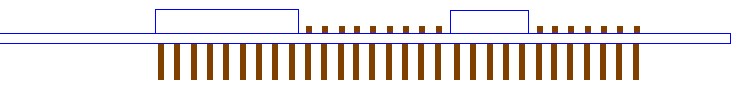
Fig: Cape board dimensions shows the outline of the standard cape. The dimensions are in inches.
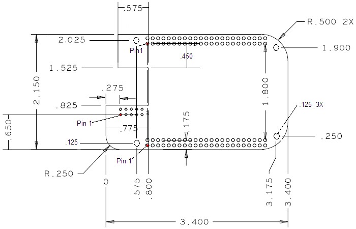
Fig: Cape board dimensions
A notch is provided for BeagleBone Ethernet connector to stick up higher than the cape when mounted. This also acts as a key function to ensure that the cape is oriented correctly. Space is also provided to allow access to the user LEDs and reset button on BeagleBone board. On BeagleBone AI-64 board align it with the notch on the board silkscreen.
Extended Cape Size
Capes larger than the standard board size are also allowed. A good example would be the new BeagleBone AI-64 robotics cape. There is no practical limit to the sizes of these types of boards. The notch is also optional, but it is up to the supplier to ensure that the cape is not plugged incorrectly on BeagleBone AI-64 such that damage would be cause to BeagleBone AI-64. Any such damage will be the responsibility of the supplier of such a cape to repair. As with all capes, the EEPROM is required and compliance with the power requirements must be adhered to.